
Link to article on Electronics Media
Chalmers University of Technology and SweGaN AB, manufacturer of custom-made GaN-on-SiC epitaxial wafers for the devices used in telecom, satellite, defense, and power electronics, announce a publication in Electron Device Letters, demonstrating new state-of-the-art results of high-voltage GaN power devices enabled by Chalmers MIS-HEMT technology and SweGaN QuanFINE buffer-free GaN-on-SiC materials.
Among key findings, the research identifies QuanFINE epiwafers as a highly competitive candidate for high-voltage power devices used for 1200V applications, in addition to its strong traction in the RF market at present.
-“With excellent results establishing the robust capability of our material, we anticipate there will be growing opportunities for SweGaN in this era of electric vehicles, where the power devices are critical for the vehicle’s performance. We are currently in discussions with early-adopter GaN power device companies to launch high-voltage power solutions that harvest the true advantages of GaN.” says Dr. Jr-Tai Chen, CTO, SweGaN.
- Paper: “High Voltage and Low Leakage GaN-on-SiC MISHEMTs on a “Buffer-Free” Heterostructure”- https://ieeexplore.ieee.org/document/9745541/
- Authors: Björn Hult, Mattias Thorsell and Niklas Rorsman, Chalmers University of Technology, Gothenburg, Sweden, and Jr-Tai Chen, SweGaN AB, Linköping, Sweden.
Sample of Abstract Highlights
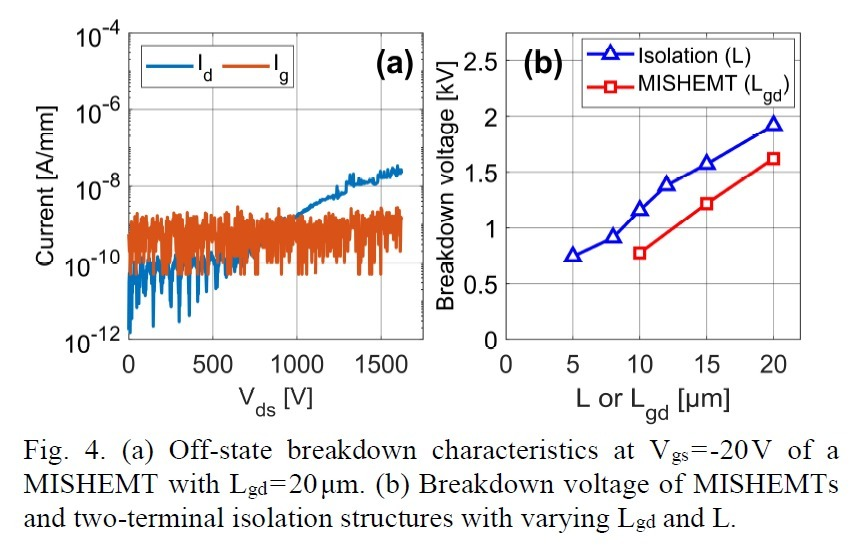
The performance of a novel ‘buffer-free’ GaN-on-SiC MIS-HEMTs for power switching applications is demonstrated in this letter. In addition, high voltage operation with exceptionally low gate and drain leakage currents is shown and specific on-resistance of 3.61 m Ω⋅ cm 2 and a breakdown voltage of 1622 V at a drain current of 22 nA/mm are achieved.
-“SweGaN has developed highly robust and innovative GaN-on-SiC materials, says Prof. Niklas Rorsman, Chalmers University of Technology. We are happy to collaborate with SweGaN on a continuous basis to perform joint research and development. The collaboration has been very successful to developing III-nitride materials and devices”
at will the key new findings mean for the GaN high-voltage market?
- Results obtained in this work demonstrated the significant potential of SweGaN’s QuanFINE® epitaxial solutions for high-voltage GaN power devices used in the applications where the performance and the reliability of the devices are both strictly required, for example, on-board chargers and power inverters of EVs
- GaN power devices available in the market have been limited up to 650V rated, due to the GaN material quality and the low-breakdown Si substrates.
- A specific on-resistance of 3.61 mΩ*cm2, an off-state breakdown voltage of over 1600 V of the MIS-HEMTs at a drain leakage current of 22 nA/mm, plus a vertical breakdown voltage of more than 3000 V were achieved. (See Figure 4)
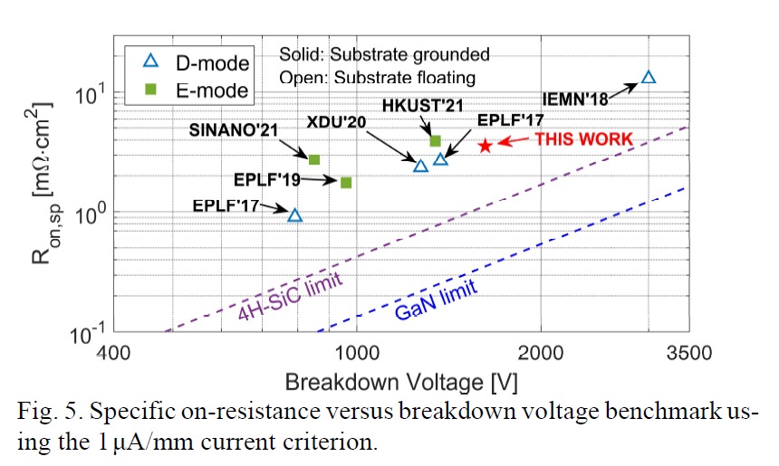
In this work, we demonstrated new state-of-the-art performance in terms of the on-resistance and the breakdown voltage of the GaN power devices fabricated on our buffer-free GaN-on-SiC materials with total epilayer thickness of roughly 20 times thinner than that of the commercial GaN-on-Si epiwafers. (See Figure 5)
“the collaboration of Chalmers and SweGaN have been successful on numerous research projects. Harnessing the combined expertise from the material level to the device level is the key behind this achievement, which will also further enhance SweGaN’s long-term market strategy and product innovation – and provide significant benefits to our global customer base,” says Jonas Nilsson, CEO, SweGaN.