QuanFine™
C-Doped
C-Doped
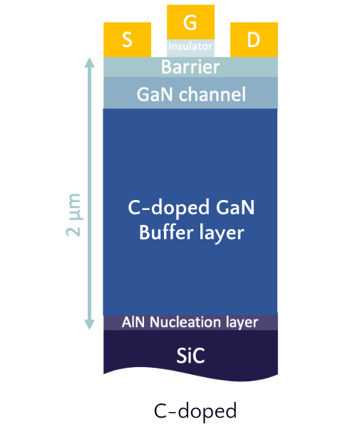
Conventional Structure
C-doping is an alternative to Fe-doping for some applications. C-doping makes the buffer semi-insulating which is necessary for the functionality of the final transistor device and is a robust alternative for achieving high breakdown voltage. The SweGaN GaN buffer is grown on our proprietary AlN nucleation layer, providing a lower thermal boundary resistance, key for improved device cooling and performance.
High breakdown voltage

Available options
Our epitaxial wafers can be highly customized according to your needs. You can see the information about the different options below. Please contact us for more information for our customization service.
| SiC wafer size | Diameter | Thickness |
|---|---|---|
| 4″ | 100 mm | 500 um |
| 6″ | 150 mm | 500 um |
| Barrier | Thickness | Composition (Al%) | Sheet resistance, Rs | Mobility, μs |
|---|---|---|---|---|
| AlGaN | 8 – 30 nm | 15 – 35 % | 250 – 400 ohm/sq | ≥ 2000 cm2/Vs |
| InAl(Ga)N | 4 – 8 nm | 83 – 89 % | 200 – 350 ohm/sq | ≥ 1700 cm2/Vs |
| AlN | 3 – 5 nm | ≥ 50 % | 280 – 250 ohm/sq | ≥ 1500 cm2/Vs |
