Link to article on Power Electronics News: January 14, 2025 Maurizio Di Paolo Emilio
In an era increasingly defined by resource scarcity and environmental challenges, innovative approaches to material reuse and recycling are paramount. The I3 CLOSER project, 70% funded by the European Union (EU), represents a bold stride toward this goal (Figure 1). This initiative seeks to reclaim and repurpose critical materials from e-waste, establishing a circular supply chain for Europe’s semiconductor industry. This article features SweGaN, a Swedish semiconductor technology company, sharing insights about the project and its role within it.
The Vision of the CLOSER Project
The CLOSER project, which stands for Circular Raw Materials for European Open Strategic Autonomy on Chips and Microelectronics Production, aims to build a European closed-loop ecosystem for semiconductors. It addresses the dual challenges of resource scarcity and reliance on non-European suppliers for critical raw materials. Funded under the European Union’s I3 program, CLOSER unites 32 partners from eight European countries, working collaboratively to develop sustainable semiconductor and microelectronics production processes.
Application objectives
- Enhance E-waste collection, sorting, and characterization through global strategies, advanced logistics, regulatory analysis, and efficient recovery of semiconductor materials, supported by innovative monitoring tools.
- Revamp obsolete electronics, reclaim SiC wafers, and implement circularity in the EU renewable energy supply chain through refurbishment, reuse, and compliance with international standards.
- Recover and refine semiconductor materials from end-of-life products and industrial scraps, ensuring high purity, traceability, and exploring their applications in modern electronics manufacturing processes.
- Upcycle e-waste by producing InP and GaAs wafers from recovered semiconductor materials, characterizing reclaimed SiC substrates, and growing secondary GaN-based HEMT epitaxial layers on SiC for RF applications.
- Produce and validate secondary chips and revamped boards by manufacturing, testing, and integrating them into new products, leveraging advanced technologies and ensuring circularity through certification and digital passport analysis.
- Develop a comprehensive Digital Product Passport for e-waste, integrating IoT and life-cycle analysis for enhanced traceability and informed decision-making in circular semiconductor manufacturing.
- Promote circular semiconducting products through communication, MOOCs, market analysis, commercial strategies, and EU collaborations
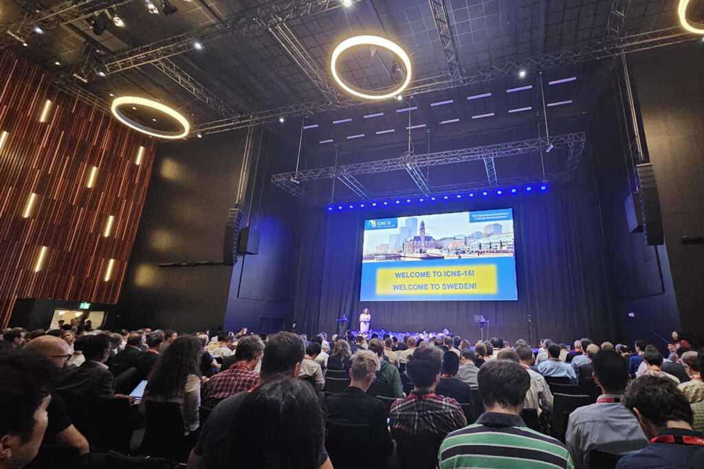
Launched officially on October 17, 2024, at the Lazio Region Administration Headquarters (Figure 2), the project will span 36 months.

SweGaN’s Role: Reclaiming Gallium and Silicon Carbide
SweGaN specializes in the production of materials for power devices, such as Gallium Nitride on Silicon Carbide (GaN-on-SiC) wafers, which are essential for high-performance electronics.
“As part of the CLOSER project, SweGaN is focusing on reclaiming critical materials like gallium and silicon carbide (SiC) wafers to reduce dependence on scarce resources and promote sustainable practices,” said Anders Lundskog, R&D Manager, SweGaN, in an interview with Power Electronics News.
Gallium Recovery and Refinement
In the CLOSER project, SweGaN will develope a method to recover gallium from waste produced during its manufacturing processes.
“Gallium is a crucial material for SweGaN’s processes, yet its availability is limited, and Europe currently lacks a domestic supplier”, said Lundskog.

He added: “This waste, which accumulates in machine filters, will be sent to specialized partners for extraction and initial refinement. From there, the material will be further purified, creating the high-purity gallium precursor required for SweGaN’s operations”.
The process is both innovative and essential. High-purity precursors are critical for semiconductor manufacturing, yet the lack of large-scale production in Europe has historically made the region reliant on non-European suppliers. By closing the loop on gallium usage, SweGaN and its partners are not only advancing sustainability but also enhancing Europe’s strategic independence in semiconductor materials.
Reclaiming Silicon Carbide Wafers
In addition to gallium recovery, SweGaN is pioneering the reclamation of SiC wafers, another critical component in semiconductor manufacturing of power RF-power devices. Partnering with Leonardo, a leading European company, SweGaN will reclaim misprocessed SiC wafers that would otherwise be discarded. Through a specialized process, SweGaN will strip the defective layers and prepare the wafers for reuse.
Fraunhofer, a renowned research institute, will assist in characterizing the reclaimed wafers to ensure they meet the stringent quality standards required for semiconductor applications. Techniques such as X-ray fluorescence, atomic force microscopy, and particle analysis will be employed to validate the integrity of the reclaimed substrates. Once qualified, these wafers will be re-coated with new GaN-on-SiC material and returned to Leonardo for device fabrication.
Challenges and Opportunities
A key challenge lies in achieving the necessary purity levels for reclaimed materials.
“While gallium recovery from machine filters is relatively straightforward, refining the metal into a high-purity semiconductor grade precursor involves complex processes that are not yet widely established in Europe. Additionally, the competitive pricing of non-European suppliers, particularly from regions like China, poses significant hurdles for local production”, said Lundskog.
Despite these challenges, the potential benefits are immense. By reducing reliance on raw material imports and decreasing waste, the project supports environmental sustainability and economic resilience. SweGaN’s efforts in gallium and SiC reclamation are expected to lower production costs, benefiting both the company and its partners, such as Leonardo.
The strategic importance of the CLOSER project extends beyond the semiconductor industry. The initiative aligns with Europe’s broader goals of reducing dependence on non-European suppliers for critical materials. Recent geopolitical developments, such as export restrictions on silicon carbide substrates by certain countries, underscore the urgency of developing domestic capabilities.
Conclusion
The CLOSER project represents a strong effort to address resource scarcity and promote sustainability in Europe’s semiconductor industry. SweGaN’s contributions, particularly in gallium recovery and SiC wafer reclamation, underscore the importance of innovation and collaboration in achieving these goals. By closing the loop on critical materials, the project not only enhances Europe’s strategic autonomy but also sets a precedent for circular practices in high-tech manufacturing.


