
Tailored Solutions On-Demand
Tailored epitaxial solutions allow customers to design and customize epitaxial solutions, based on individual technical requirements.
Customizing your epitaxial solutions
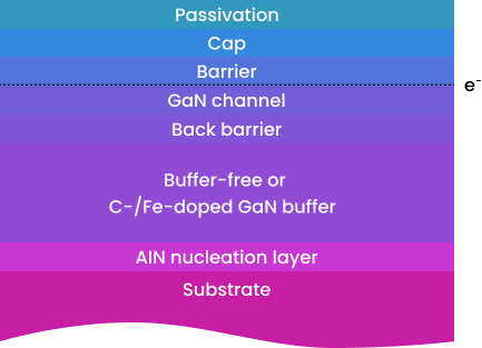
SweGaN offers tailored epitaxial solutions on-demand to address specific technical challenges and fulfill bespoke requirements. Creating customized epitaxial solutions starts by selecting from a range of substrates and options for Buffer, Barrier, Cap, Passivation and Back Barrier.
Reach out to our specialists to explore additional customization options based on your needs.
Customization
SUBSTRATE
- 3’’/4’’/6’’ SiC
- GaN
- Sapphire
- Silicon
Buffer
The conventional Fe-doped or C-doped buffer layer offers great compatibility with existing RF/power transistor technologies. Our unique buffer-free epitaxial solutions enable exceptional device performance and reliability without noticeable trade-offs.
- Buffer-free (channel)
- Fe-doped buffer
- C-doped buffer
Barrier
The barrier layer not only induces the channel electrons (e–), but also serves as a critical layer that defines the transistor technology. We provide a wide range of barrier layers for different transistor technologies.
Options:
- AlGaN
- AIN
- InAIN
- InAIGaN
Cap
The cap is typically a thin GaN layer, which alleviates the oxidation of the barrier, improving the reliability of the devices. For normally-off devices, a thick GaN layer is needed with Mg-doping to fully deplete the channel electrons.
- UID GaN
- Mg-doped GaN
Passivation
- In-situ SiNx
- Ex-situ SiNx
BACK Barrier
The back layer is typically employed in a HEMT structure for highly scaled devices to further improving the electron confinement and minimizing the short channel effects.
- AlGaN
- Al(Ga)N/Ga(Al)N superlattice
Reach out to discuss your technical needs and learn more Tailored Solutions On-Demand from SweGaN’s experts