SweGaN excels in the epitaxial growth of III-nitride semiconductors, leveraging a broad range of epitaxy technologies to master interface engineering, epitaxial layer growth, and structure design.
QUANFINE®
A new generation of GaN HEMT epitaxial solutions
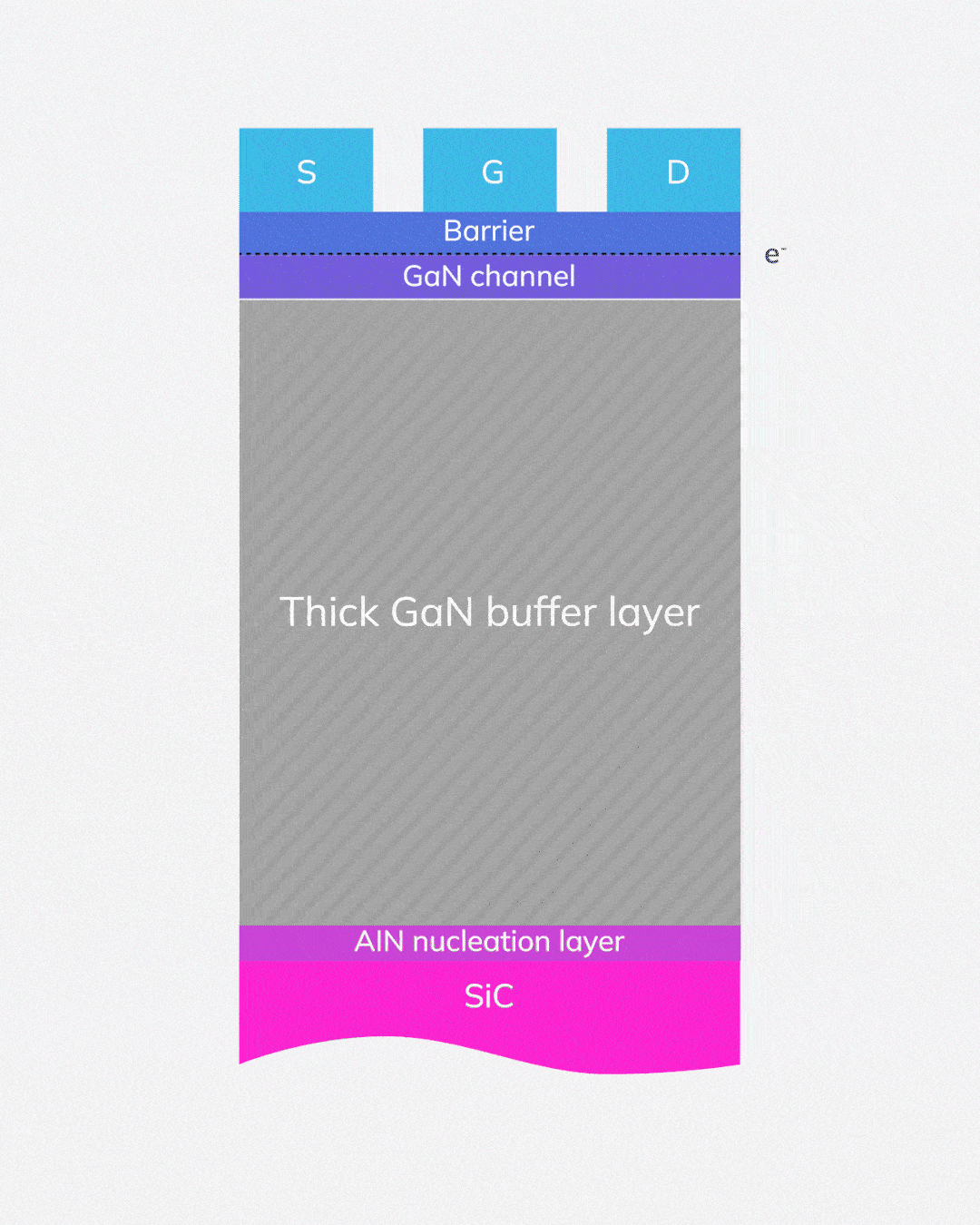
SweGaN’s unique QuanFINE® structure is developed based on a buffer-free concept that seamlessly combines the strengths of GaN and SiC, WITHOUT the conventional thick C-/Fe- doped buffer layer. The buffer-free structure is realized by a revolutionary epitaxial process including “Transmorphic Heteroepitaxy, “ where vacancy ordering is involved to perfectly transform the in-plane lattice atomic configuration from the SiC substrate to the AlN nucleation layer.
QuanFINE® brings the hot channel closer to the heat-sink SiC substrate, eliminate the high-density dislocations in the buffer, reduce the buffer-related traps, and use the ultra wide-bandgap AlN nucleation layer as an effective back-side barrier.
Providing superior material quality and characteristics, QuanFINE® enables a superior level of device performance and reliability for both RF and power applications.
Up to 10% higher power efficiency
Up to 25% higher power density
Up to 2X higher breakdown strength
The lowest thermal resistance in class
The best linearity in class
Record-high electron mobility
SweGaN’s proprietary high-mobility growth process enables higher efficiency, power density, and higher operation frequency of transistors. The channel electron mobility is enhanced by 20-30% higher as a result.
20-30% higher electron mobility
State-of-the-art structural quality
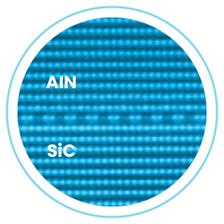
GaN and AlN epitaxial layers grown using SweGaN’s high-temperature process exhibit excellent structural quality, where typically, threading dislocation density in the GaN layer is in the low 108 cm-2 regime and the AlN nucleation layer is free of grain boundaries. This best-in-class structural quality guarantees GaN robustness and dramatically reduce the risk of device failure due to the structural defects.
Excellent structural quality at atomic level
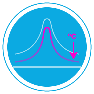
Ultra-low thermal boundary resistance
The conventional thermal boundary resistance (TBR) in the GaN – SiC interface causes up to 40% additional channel temperature rise in transistors. Using our ultra-low TBR AlN nucleation layer, the additional temperature rise is minimized, making the temperature of the transistor much colder than the one built on conventional GaN on SiC materials.