QuanFine™
Fe-Doped
Fe-doped
There are many variations of passages of Lorem Ipsum available, but the majority have suffered alteration in some form, by injected humour, or randomised words which don’t look even slightly believable. If you are going to use a passage of Lorem Ipsum, you need to be sure there isn’t anything embarrassing hidden in the middle of text.
Conventional Structure
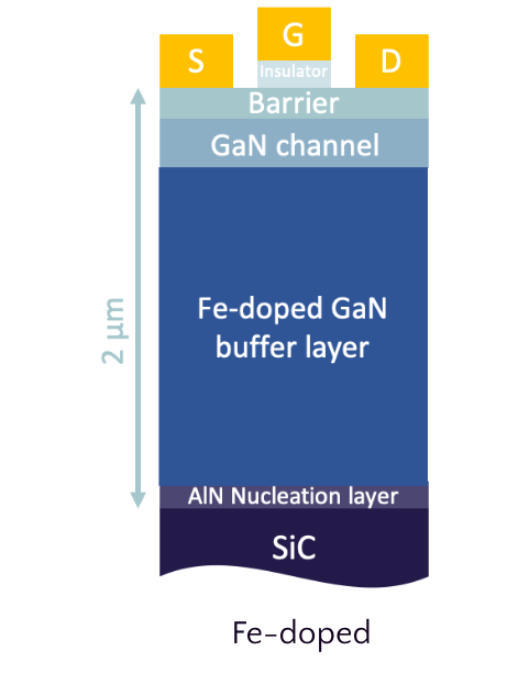
The industry standard, Fe-doped GaN epi-wafer, high-electron, mobility transistor structure is highly popular standard for telecommunication devices – such as those found in radio base-stations and satellites. Using this structure, you receive a GaN buffer with Fe acceptors that make the GaN buffer highly resistive, i.e., low leakage current, and provides a high-power density. This Fe-doped structure is grown on our proprietary AlN nucleation layer, which provides enhanced thermal conductivity for improved device cooling and performance.
Our Fe-doped material has been benchmarked and fully validated. It features high-power density and other characteristics that are comparable with the state-of-the-art Fe-doped material.
High power density

Available options
Our epitaxial wafers can be highly customized according to your needs. You can see the information about the different options below. Please contact us for more information for our customization service.
| SiC wafer size | Diameter | Thickness |
|---|---|---|
| 4″ | 100 mm | 500 um |
| 6″ | 150 mm | 500 um |
| Barrier | Thickness | Composition (Al%) | Sheet resistance, Rs | Mobility, μs |
|---|---|---|---|---|
| AlGaN | 8 – 30 nm | 15 – 35 % | 250 – 400 ohm/sq | ≥ 2000 cm2/Vs |
| InAl(Ga)N | 4 – 8 nm | 83 – 89 % | 200 – 350 ohm/sq | ≥ 1700 cm2/Vs |
| AlN | 3 – 5 nm | ≥ 50 % | 280 – 250 ohm/sq | ≥ 1500 cm2/Vs |