QuanFine™
QuanFINE®
The new generation of GaN
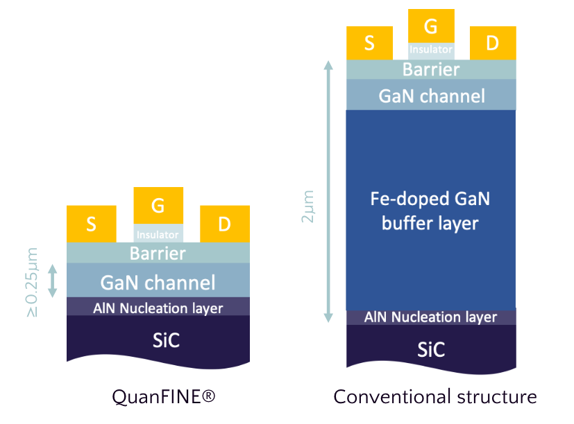
QuanFINE® is the new generation of GaN high-electron mobility transistor structure that is an order of magnitude thinner than conventional structures. Providing superior material quality and improved thermal transfer, QuanFINE facilitates devices by enabling both higher switching frequencies and power densities. Our unique technology enables us to achieve this level of performance without added epi-wafer cost while also providing lower power consumption and reduced system complexity, ultimately furnishing significant benefits for manufacturers. Furnishing superior reliability, the SweGaN QuanFINE structure can be used in both development of cutting-edge telecommunication devices for applications like satellites and 5G base-stations, and for high power devices, such as those found in supercharging systems for electric cars.
Unique buffer free structure
QuanFINE® structure is built on a concept of GaN-SiC hybrid material, that combines the high-electron-velocity thin GaN with the high-breakdown-voltage bulk SiC. By removing the conventional thick doped buffer layer, we are able to bring the hot channel closer to the heat-sink SiC substrate, eliminate Fe-related deep traps, and shorten the production time.
300% Higher breakdown voltage
30% Higher power density
50% Lower thermal resistance
1000% Lower memory effect
50% Lower current collapse

Record-high electron mobility
SweGaN’s record-high channel electron mobility enables higher efficiency and higher operation frequency of the transistors. Using SweGaN’s proprietary high-mobility growth process, the channel electron mobility is 20-30% higher than the conventional channel electron mobility. The record-high mobility enables higher efficiency and higher operation frequency of the transistors.
State-of-the-art structural quality
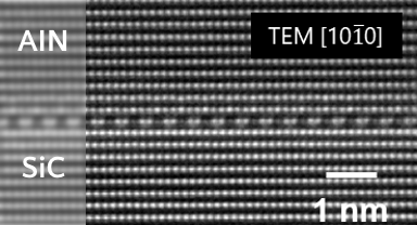
GaN and AlN epitaxial layers grown by SweGaN’s high-temperature process exhibit excellent structural quality. Typically, the threading dislocation density in the GaN layer is in low 108 cm-2 regime and the AlN nucleation layer is free of grain boundaries. This is the best structural quality in the class, which not only guarantees the GaN robustness but also dramatically reduces the risk of device failure due to the structural defects.

Ultra-low thermal boundary resistance
The conventional Thermal Boundary Resistance (TBR) in the GaN – SiC interface causes up to 40% additional channel temperature rise in transistors. Using our ultra-low-TBR AlN nucleation layer, we have been able to reduce this additional temperature rise to a negligible level. The outstanding structural quality of the thin AlN nucleation layer significantly improves the heat transport from the channel down to the high-thermal-conductivity SiC substrate. This allows us to address one of the biggest challenges with RF and power devices: reliability. By reducing the operational temperature by 25 °C, the device lifetime is increased by a factor of 10.
Available options
Our epitaxial wafers can be highly customized according to your needs. You can see the information about the different options below. Please contact us for more information for our customization service.
| SiC wafer size | Diameter | Thickness |
|---|---|---|
| 4″ | 100 mm | 500 um |
| 6″ | 150 mm | 500 um |
| Barrier | Thickness | Composition (Al%) | Sheet resistance, Rs | Mobility, μs |
|---|---|---|---|---|
| AlGaN | 8 – 30 nm | 15 – 35 % | 250 – 400 ohm/sq | ≥ 2000 cm2/Vs |
| InAl(Ga)N | 4 – 8 nm | 83 – 89 % | 200 – 350 ohm/sq | ≥ 1700 cm2/Vs |
| AlN | 3 – 5 nm | ≥ 50 % | 280 – 350 ohm/sq | ≥ 1500 cm2/Vs |
